3.5 KiB
Node Design
Design Process (led by sietse)
Thoughts
Before making the design i was thinking about the following things:
- The node should be compact and simple
- The node should have a screen
- The node should have a bar with led's to show how much sound is picked up on the node
- The node should have a hexagon grid where the sensors are located behind
- The node should have two lights on top
- The nodes should be powered by batteries
I also thought about the following things on how to make the design. I have decided to make the design using fusion360, because i have some experience with it and i think it is a good tool to make the design. I wanted it to be really easy to assemble so i split the design in two parts. The top and the bottom. The top part will be the part with the screen and the sensors, and the bottom part will be the part with the whole circuitboard.
Bottom design
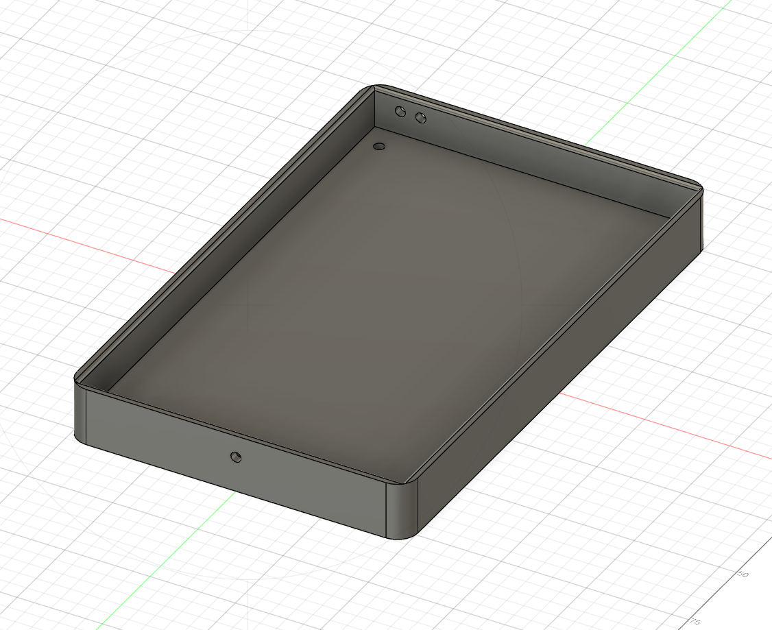
I made the final design of sprint 1 using fusion360. I used the original drawing from Bram and modified it using the feedback we've got from the usertest. I begun making the bottom side of the node, because this could serve me as a template to make the rest. The bottom side was pretty easy to make because i only had to sketch and measure a few things. It eventually looked like this:
Top design
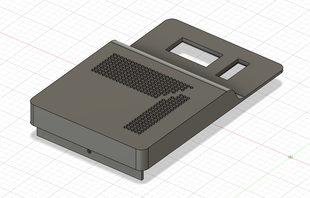
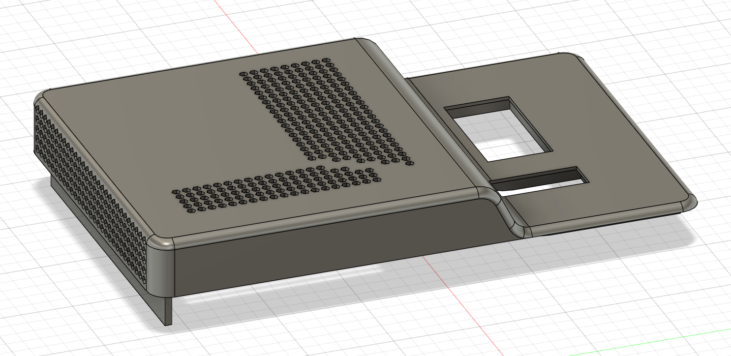
When i went to work on the upper side it took some more time than the bottom one. since i had to make cutouts for the screen and led bar and the hexagon grid. The hexagon grid was the hardest because i used the geometric pattern fucntion on my hexagon object and i had to make sure that there would still be room between the hexagons. I made it so the screens have like a indent on the top part. Otherwise the battery, sensors and esp32 wouldnt be able to fit underneath the grid. The final product looks like this:
Assembly
First assembly
The part was finished on 15/2 at 11am. I first screwed the pcb in the bottom part which was really easy to do. When trying to put the top part on the bottom part i noticed that the holes were not aligned, and the batteryholder was fatter than i thought. I tried to cut some material away from the top part but it was still not fitting.
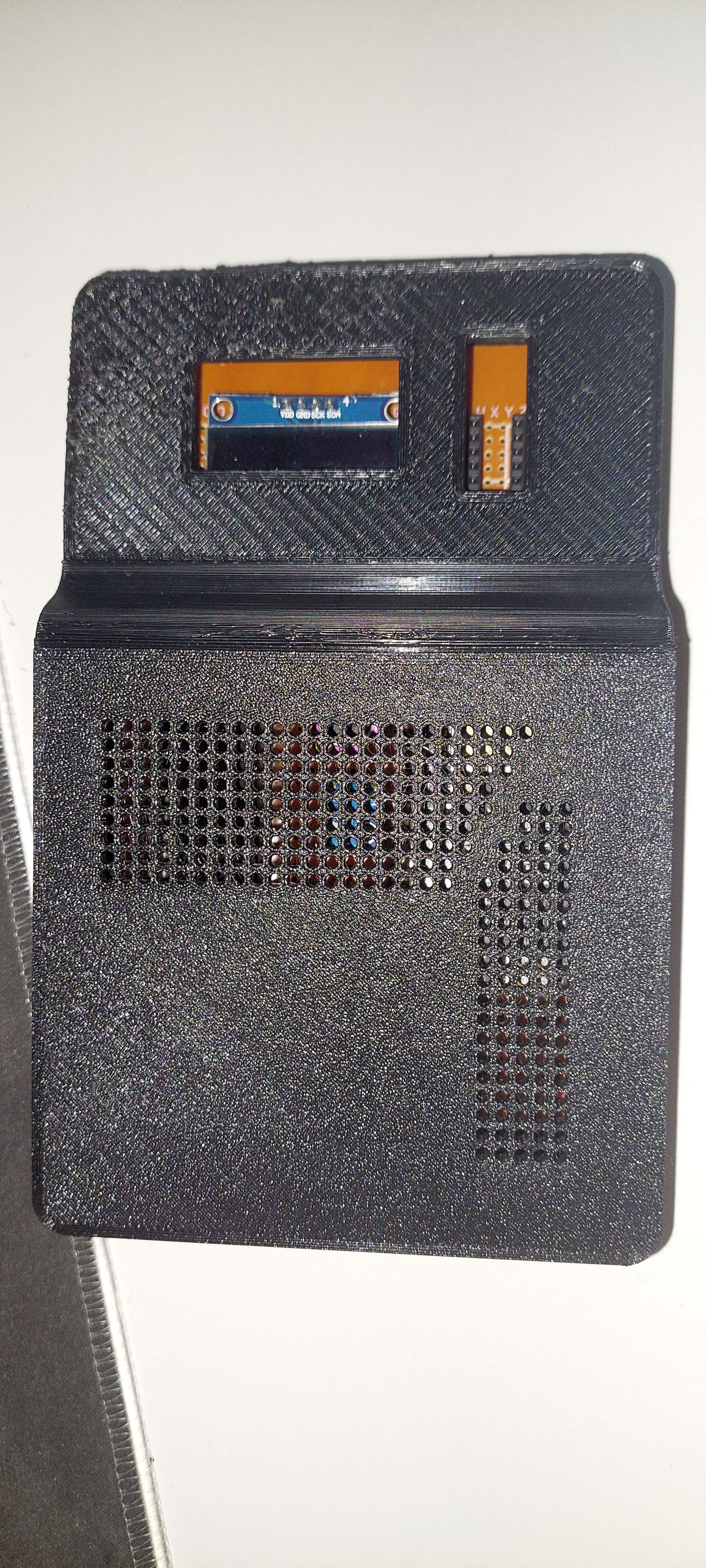
It looked like this from the top:
You can see that the oled screen cutouts and the led bar cutouts are not aligned with the components on the pcb.
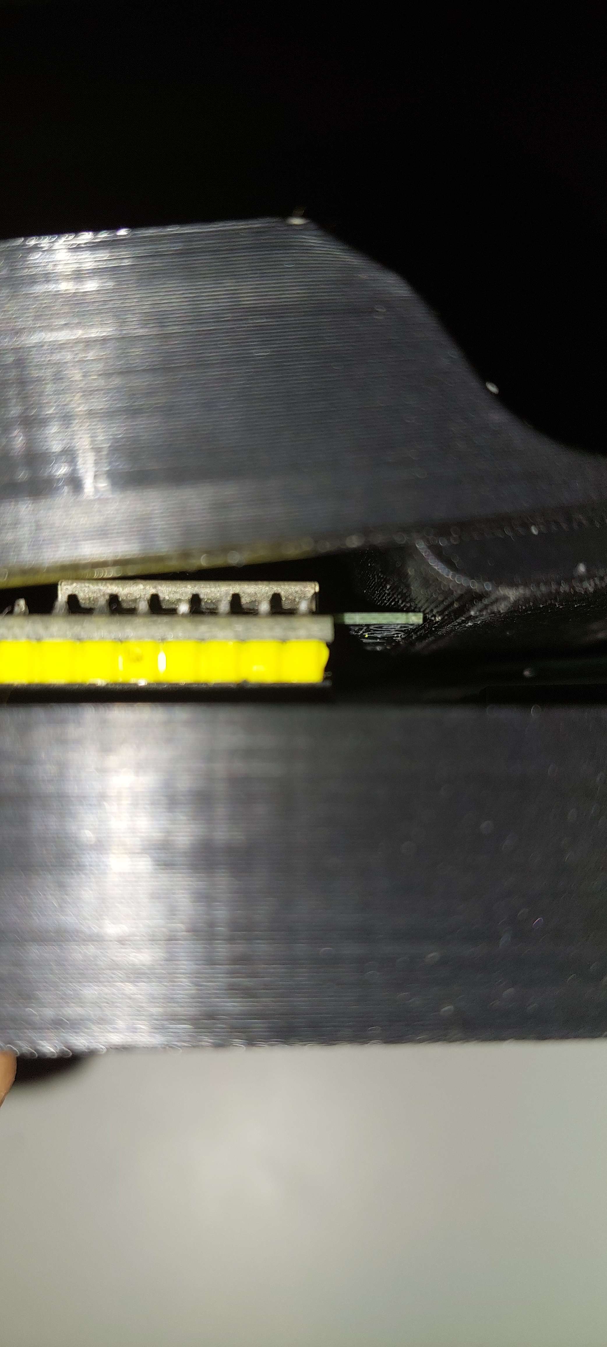
And like this from the side view:
Here you can see that the wifi antenna of the esp32 is not fitting in the top part, because the fillet is too small.
Second assembly
In fusion360 i made the cutouts for the screen and the led bar lower on the part. I also made the fillet on the top part a bit bigger, and adjusted the fillet on top too. We also decided we'd take this oppurtunitty to make vent holes in the bottom aswell. This is because hot air rises and with this there would be a little bit of air coming through the node for more accurate readings. I then printed the new design and it took around 7 hours. The new design looks like this:
The new design fits perfectly and looks like this:
...
Conclusion
graph LR
A[Design Sketch] -->|Usertest| B(Fusion360 design)
B -->|Not fitting| C[New fusion360 design]
C -->|assembly| D[Finished product]
